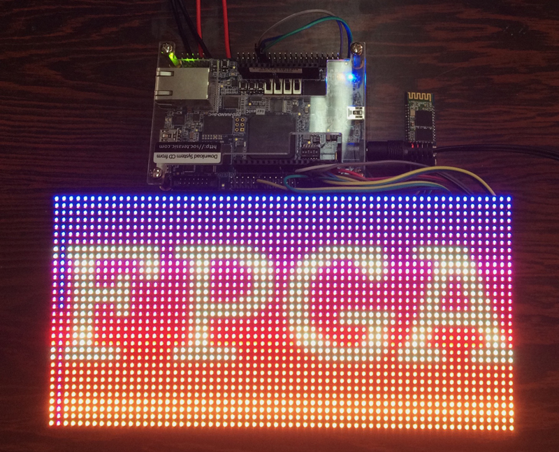
Dot matrix displays are an elegant way to display images or messages. However, a lot of signal pins are needed to drive those displays and they are quite power hungry. A very high framerate can thus be achieved, as will be shown below, using an FPGA.
So first of all, the display used for this example is a 64x32 RGB LED dot matrix display. It is powered by 5V and draws over 4.5A at full brightness. As LED constant current drivers are used though, I have experimented on dropping the input voltage down to 4.3V, without a brightness descrease (achieving a 15% reduction of power use).
To drive the display the following signals need to be supplied:
- Four signals which select the row couple (0-15).
- Three signal couples (RGB1 and RGB2) which select if each LED will be activated or not.
- A clock signal for the shift register.
- A latch enable signal for the shift register.
- An output enable signal.
All in all, this makes 13 different signals that need to be provided. Furthermore, in order to achieve a high framerate, the clock frequency needs to be quite high (several MHz) since this is a 64x32 display. Therefore, a microcontroller with a high clockrate could be used, or, in this case, an FPGA.
So in this example a Terasic DE0 Nano SoC is used, which gets the image via Bluetooth from the computer and displays it.
The display works as follows: Each time, only one row couple is activated, selected by the row signals (i.e. row 0 and 16, row 1 and 17, row 2 and 18 etc.). So the high refresh rate is essential, as otherwise the switching of each row would be visible. For each row couple, the RGB value of each column is clocked serially, using a shift register. After 64 clock cycles, using the latch enable (LE) signal, the new data is activated for the selected rows. The output enable signal (OE) which is active low is used when the row is changed, because the transistors which activate each row have a high settling time. The LED drivers either activate or deactivate each LED. So for a controlled brightness, the ON time must be modulated, just like PWM.
So, to implement all of the above on the FPGA the following modules are used. A UART module (to get the data from the computer), the main matrix controller and a dual-port access RAM.
Beginning with the main matrix controller, it reads the data from the RAM and generates the appropriate signals. Each color has an 8-bit brighness value. In order limit the amount of data transmitted, for the PWM, only 8 different levels are used (instead of 256), corresponding to the 8 different bits of each color. The ON time of each level is proportional to the significance of each bit (meaning 1, 2, 4, 8,...,128).
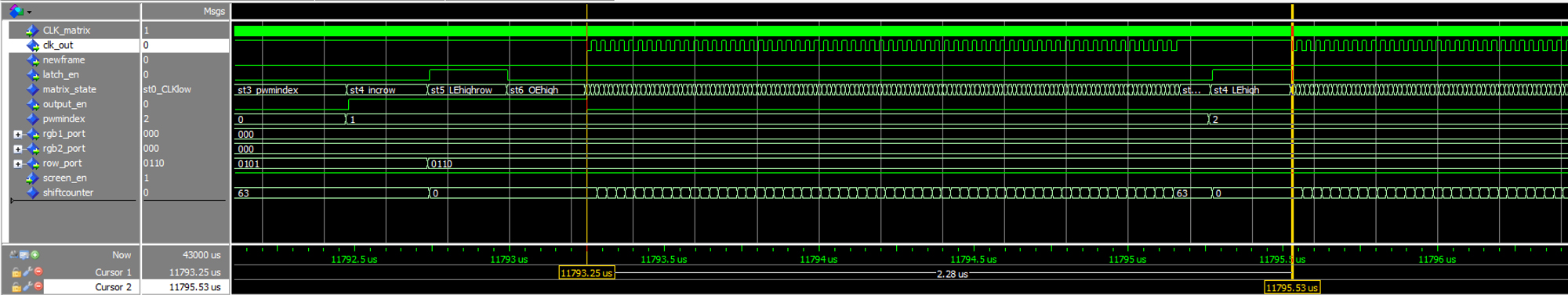
In more detail, a simulation of the different signals is shown below. The clk_out signal is the shift register clock, whereas the CLK_matrix is the component clock (200MHz, generated using a PLL). The 64 clock cycles are shown, after the latching of the previous group. The timing unit (meaning the smaller ON time for each LED) is 2.28us.
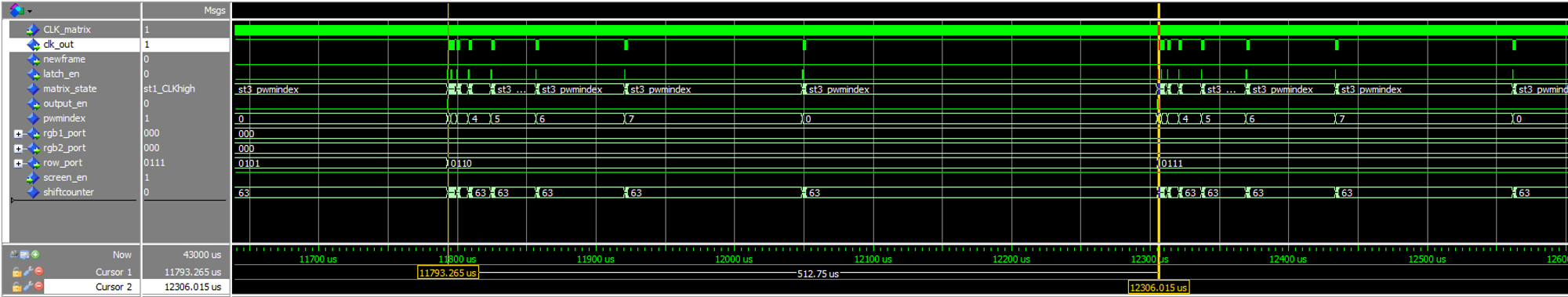
Zooming out, the modulation for each row can be seen. After each latching, the next group is loaded to the shift register, waiting for the next latch enable. The different latch times can be seen. So, a 64column row, with 8 different bytes (256 levels) for each color needs 512.76us in order to be updated.
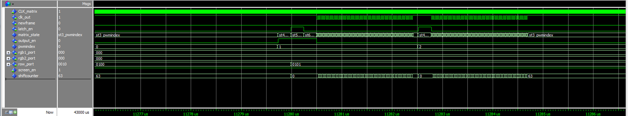
After the row is complete, before moving to the next row, the row signal (row_port) needs to be updated and latched. During this time, the output is deactived (output_en is high).
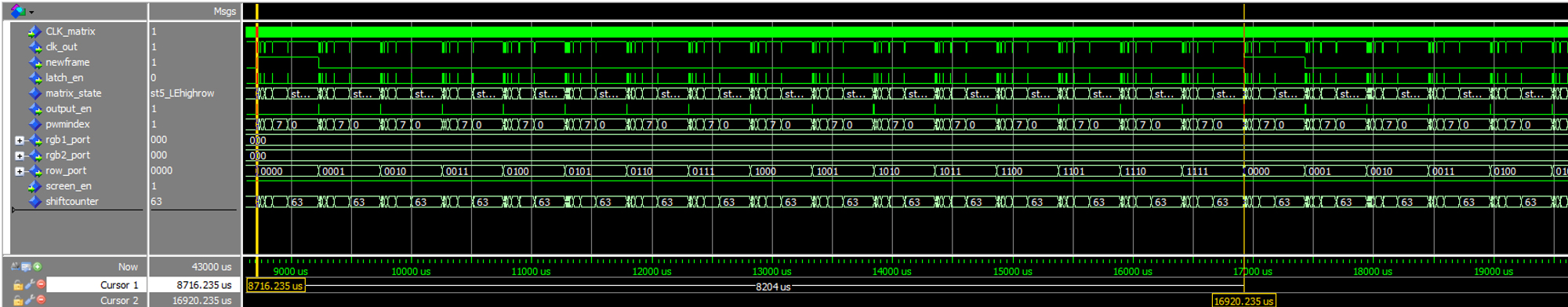
Finally, the following figure displays an update of a complete frame. It takes 8.204ms for a full frame update, which translates to over 120fps refresh rate.
The value for each LED is provided from the UART module and saved on the RAM module. So dual-port access RAM is used for simultaneous read/writes. Since the UART protocol is not capable of supplying new data on such a high bit-rate, the RAM module has twice the space needed. So as the first half of the RAM is filled with new data from the computer, the image saved on the second half of the RAM is displayed and vice versa.